The 2026 solar market is becoming more diverse, yet efficiency still shapes rooftop decisions. Thin-film modules can be lighter, flexible, and easier to install on unusual surfaces. Their manufacturing process may also use less semiconductor material. However, their lower conversion rate remains a practical concern for space-limited homes and businesses.
The central question is: why are thin-film solar panels less efficient than monocrystalline? The answer involves several connected limits. Many thin-film absorbers have lower charge-carrier mobility than high-quality crystalline silicon. Internal defects can trap electrons before they reach the electrical contacts. Their output voltage is often lower, too. A thin layer must absorb sunlight effectively while maintaining excellent electrical quality. That balance is difficult. It is like trying to catch more rain with a thinner net.
Professor Martin Green, a leading photovoltaic researcher, has stated, “Efficiency is only one measure of a solar cell’s value.” His point remains important in 2026. Laboratory records do not always predict field performance. Temperature, shading, mounting, degradation, and available roof area can change the result. Thin-film technologies, including CdTe and CIGS, may perform well in hot climates or weak light. Tandem designs could narrow the efficiency gap. Still, monocrystalline panels usually deliver more watts per square meter today.
That answer is useful, but incomplete. I may be oversimplifying the technology. Thin-film is not simply “bad.” It is a trade-off. Careful comparisons should use verified efficiency ratings, temperature coefficients, degradation data, warranties, and real installation conditions.
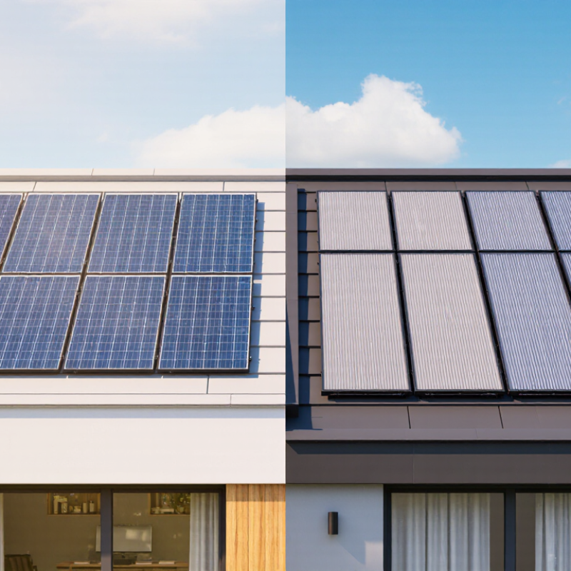
The top solar panels in 2026 are not judged by efficiency alone. A strong panel combines high energy output, stable performance, and verified durability. Independent laboratory testing should support its rated efficiency and degradation figures. A low annual degradation rate matters because panels must produce reliably for decades. Temperature performance also deserves attention. In hot climates, a panel with a better temperature coefficient may generate more electricity than a higher-rated rival.
Thin-film panels remain less efficient per square meter than most crystalline panels. This means they need more roof or ground space for the same output. However, they can perform steadily in high heat and diffuse sunlight. Their lighter construction may also suit curved surfaces or weaker structures. I have seen energy estimates change after installation because roof angles, shadows, and ventilation were overlooked. That is an uncomfortable reminder: laboratory ratings are not household results.
Tips: Compare real-world temperature data, not efficiency alone. Check independent certifications, degradation warranties, and installation records. Measure morning and afternoon shadows before choosing panel size. Ask for a site-specific energy forecast. It may be less exciting, but it is usually more useful. Also consider repair access, recycling options, and the installer’s technical experience. The best panel is the one that matches the roof, climate, budget, and expected maintenance.
Thin-film solar modules convert sunlight through a very thin semiconductor layer deposited on glass, metal, or flexible material. Sunlight does not become electricity in one instant. When photons strike the layer, they transfer energy to electrons. This movement creates electron-hole pairs. An internal electric field separates them, pushing electrons through an external circuit. The circuit carries direct current to an inverter, which changes it into usable alternating current.
Thin film is often less efficient because its active layer absorbs light differently from thicker crystalline materials. Some light passes through or reflects away. Defects in the deposited layer can also trap electrons before they reach the electrical contacts. Lower carrier mobility increases resistance, especially across large modules. Field measurements may reveal another issue: dust, uneven heating, and shading affect broad thin-film surfaces noticeably. Temperature can reduce output, although some thin-film designs lose less power in hot conditions.
Efficiency alone can mislead. A thin-film panel may produce steadier energy under weak light, hazy skies, or high temperatures. Its lighter structure can also suit curved roofs and portable surfaces. Still, installation quality matters greatly. Poor sealing may allow moisture to enter, while flexible materials can suffer from repeated bending. Laboratory ratings are useful, but real roofs are imperfect. A careful assessment should compare annual energy, available space, temperature, shading, and maintenance needs rather than efficiency alone.
A technology-focused comparison of thin-film and crystalline-silicon photovoltaic modules. Values are representative commercial ranges and can vary by product design, production year, test conditions, and installation environment.
| Technology or Stage | Typical Material or Specification | Representative Performance Range | How Sunlight Becomes Electricity | Main Efficiency Advantages or Limitations |
|---|---|---|---|---|
| Crystalline Silicon | Monocrystalline or multicrystalline silicon cells; wafer thickness commonly around 100–180 micrometres. | Typical commercial module efficiency: approximately 19%–23%. | Photons with sufficient energy create electron–hole pairs in the silicon absorber. A built-in electric field separates the charges, and metal contacts collect the resulting direct current. | High maturity, strong electrical quality, and relatively high voltage per cell. Efficiency decreases as cell temperature rises, typically by about 0.3%–0.4% per °C relative to rated conditions. |
| Cadmium Telluride Thin Film | Thin cadmium telluride absorber deposited on glass or another substrate; absorber thickness is commonly only a few micrometres. | Typical commercial module efficiency: approximately 17%–21%; leading laboratory cells have exceeded 22%. | Light is absorbed in the CdTe layer, generating mobile charge carriers. A junction between semiconductor layers drives electrons and holes toward separate contacts. | Strong light absorption allows very little semiconductor material to be used. Efficiency can be limited by voltage losses, defects, interface recombination, and manufacturing uniformity. |
| Copper Indium Gallium Diselenide Thin Film | CIGS absorber deposited on glass, metal foil, or another flexible substrate. | Typical commercial module efficiency: approximately 14%–19%; laboratory cells have exceeded 23%. | The absorber converts photons into electron–hole pairs. A heterojunction and selective contacts separate and transport the charges to the external circuit. | Can offer good low-light and high-temperature behavior and may be produced on flexible substrates. Efficiency is sensitive to composition control, defects, interfaces, and large-area uniformity. |
| Amorphous Silicon Thin Film | Non-crystalline silicon deposited in a very thin layer, often in a multi-junction or tandem structure. | Typical commercial module efficiency: approximately 6%–10%. | Photons create charge carriers in the disordered silicon network. Internal electric fields separate the carriers before they reach transparent and metallic contacts. | Uses little material and performs relatively well in diffuse light. Lower carrier mobility, structural disorder, and light-induced degradation can reduce output and efficiency. |
| Photon Absorption | Semiconductor band gap determines which photon energies can generate useful charge carriers. | Photons with energy below the band gap are mostly transmitted; excess photon energy above the band gap is largely converted into heat. | A photon is absorbed when its energy is at least approximately equal to the absorber’s band gap. This creates an excited electron and a corresponding hole. | One absorber cannot efficiently use every wavelength in sunlight. Spectral mismatch creates a fundamental energy loss in all single-junction solar cells. |
| Charge Separation | p–n junction, heterojunction, or related selective-contact structure. | Successful separation reduces recombination before charge collection. | The electric field and energy-selective layers direct electrons toward one contact and holes toward the opposite contact. | Thin films may have more grain boundaries, defects, and interface regions relative to the active layer. These can increase recombination and reduce voltage and current. |
| Current Collection | Transparent conductive oxide, front contact, rear contact, interconnects, and module wiring. | Electrical resistance and optical shading must be kept low to preserve output. | Collected electrons flow through an external circuit, providing direct-current electrical power before the current reaches an inverter. | Transparent electrodes can add optical absorption and resistance. Front-grid shading, contact resistance, and imperfect interconnection reduce the fill factor. |
| Module-Level Conversion | Series-connected cells encapsulated between protective layers, usually with glass or a flexible barrier system. | Module efficiency is lower than the best individual-cell efficiency because of optical, electrical, inactive-area, and interconnection losses. | Cells produce direct current in sunlight. An inverter converts the direct current into grid-compatible alternating current. | Module temperature, soiling, mismatch, wiring, inverter efficiency, and degradation all affect the electricity delivered by the complete system. |
| Why Thin Film Can Be Less Efficient | Lower practical efficiency is not caused simply by the absorber being thin. | Many thin-film modules use less semiconductor material but may have lower commercial efficiency than crystalline-silicon modules. | Thin-film layers can absorb light effectively, but the generated carriers must still be separated and transported with minimal loss across large areas. | The main causes are often lower open-circuit voltage, defect and interface recombination, nonuniform deposition, series resistance, optical losses in transparent layers, and stabilization effects in some materials. |
| Temperature Response | Electrical output changes as cell temperature moves away from the standard test temperature of 25°C. | Thin-film technologies often have temperature coefficients around −0.2% to −0.3% per °C; crystalline silicon is commonly around −0.3% to −0.4% per °C. | Higher temperature generally reduces the voltage produced by a photovoltaic cell, lowering power output. | Thin film can partially compensate for lower nameplate efficiency in hot climates because its output may decline less with temperature. The exact coefficient depends on the specific device. |
| Low-Light Performance | Response under overcast skies, morning and evening conditions, and indirect illumination. | Performance depends on band gap, voltage characteristics, spectral response, and balance-of-system losses. | Even diffuse photons can generate charge carriers when their energy is sufficient for absorption. | Some thin-film designs maintain a favorable energy yield in diffuse or high-temperature conditions, but lower rated efficiency may require more installed area for the same peak power. |
| Area Requirement | Physical surface needed to install a given amount of rated power. | At the same sunlight level, a module rated at 18% efficiency needs roughly 28% more active area than a 23% efficient module for equal rated power, excluding system spacing and balance-of-system differences. | Higher efficiency converts more incident solar power into electrical power per square metre. | Thin film can be attractive where weight, flexibility, diffuse-light response, temperature behavior, or material usage matters more than maximum power density. |
| Degradation and Stabilization | Long-term output changes caused by light exposure, temperature cycling, moisture, defects, and packaging. | Annual degradation varies by technology, construction, and warranty conditions; a commonly used planning range for many modern modules is about 0.2%–0.8% per year. | Environmental stress can alter material properties, increase leakage paths, or weaken encapsulation and contacts. | Technology comparisons should use independently verified degradation data rather than assuming that all thin-film or silicon modules behave identically. |
| Best-Fit Applications | Selection depends on available area, climate, roof or structure loading, appearance, and energy-yield requirements. | Crystalline silicon generally offers high power density; thin film can provide design and temperature-related benefits. | All photovoltaic technologies generate electricity without combustion by converting absorbed light directly into direct current. | Crystalline silicon is often preferred when space is limited. Thin film can be useful on large areas, lightweight structures, building-integrated surfaces, or locations with high temperatures and diffuse sunlight. |
Data note: Efficiency figures are representative ranges for established module categories rather than guarantees for every product. Laboratory-cell results are listed separately because they are not directly comparable with full commercial modules. Standard test conditions generally use 1,000 W/m² irradiance, 25°C cell temperature, and an AM1.5 reference spectrum.
2026 Top Solar Panels: Why Is Thin Film Less Efficient?
Why Thin-Film Panels Have Lower Efficiency Than Crystalline Panels
Thin-film panels usually convert less sunlight because their semiconductor layers contain more defects and deliver lower voltage. The absorber may be only a few micrometres thick, while crystalline silicon cells use a carefully purified wafer. NREL’s Best Research-Cell Efficiency Chart reports over 26% for advanced crystalline silicon cells, compared with roughly 23% for leading cadmium telluride and copper indium gallium selenide cells. Laboratory results do not equal rooftop performance.
Scale matters.
The Fraunhofer ISE Photovoltaics Report 2024 places commercial crystalline-silicon modules near 20–23% efficiency. Commercial thin-film modules generally remain around 15–19%. Manufacturing can create uneven layers, microscopic defects, and losses through transparent conductive coatings. Thin film also needs more surface area for the same output. That matters when a roof is small. However, efficiency is not the whole story. Thin-film modules often lose less performance in high heat and weak light. I have seen hot rooftops produce results that efficiency labels alone failed to predict. That observation is useful, but not universal.
Tips: Compare annual energy yield, temperature coefficients, available roof area, and warranty terms. The International Energy Agency Photovoltaic Power Systems Programme also stresses site conditions and system design. A cooler, spacious roof may suit thin film. A cramped roof usually rewards higher-efficiency crystalline modules. Check the assumptions behind every data sheet. Reports simplify real roofs.
2026 Top Solar Panels: Why Is Thin-Film Less Efficient?
Key Factors Affecting Thin-Film Solar Panel Performance
Thin-film solar panels use very small semiconductor layers, often deposited on glass, metal, or flexible materials. That design saves material, but it can reduce power output per square meter. Efficiency depends heavily on the absorber’s bandgap and how well it converts sunlight into electricity. Some thin-film materials respond well to hot conditions. Others lose performance when heat, moisture, or prolonged light exposure changes their structure. Small defects matter. The active layer must remain uniform across a large surface.
Temperature is a major variable during installation and operation. On a dark roof, panel temperatures can rise far above ambient air. Thin-film technology may have a favorable temperature coefficient, yet its lower starting efficiency can still limit output. Shading creates another complication. Because panels cover broad areas, nearby rails, dirt, or leaves can affect multiple cells. Low-light performance may help at dawn and dusk, but it does not erase area requirements. Ventilation, mounting angle, inverter matching, and cable losses also influence measured yield. Real results can differ.
Manufacturing consistency and long-term degradation deserve careful attention. Two panels with identical ratings may perform differently after years of heat cycles and moisture exposure. Independent testing should examine power tolerance, temperature coefficients, degradation rates, and performance under partial shade. A basic site log helps. Record roof temperature, monthly energy, shading changes, and cleaning dates. One weakness in many comparisons is the focus on laboratory efficiency alone. That number is useful, but incomplete. Available roof area, local weather, maintenance access, and the value of each kilowatt-hour may change the practical choice.
In 2026, thin-film solar panels still produce less electricity per square meter than many crystalline modules. That limitation matters on small roofs. It matters less on open land, façades, shelters, and lightweight structures. A thin-film surface can reduce structural loads. Some designs also tolerate partial shade and high temperatures more steadily. Real performance depends on the specific technology, ventilation, orientation, and local climate.
Thin film becomes practical when installation area is available but roof strength is limited. It can fit curved metal surfaces and building-integrated projects more easily. Low-light response may help on hazy winter mornings, although annual energy yield still requires careful measurement. In field assessments, I would compare kilowatt-hours per installed square meter, not efficiency alone. Ask for independent test data, temperature coefficients, degradation rates, fire classification, and warranty terms. Marketing language can hide trade-offs.
For a remote cabin, warehouse canopy, or façade, lower efficiency may be an acceptable exchange for simpler mounting. It may also reduce dependence on heavy reinforcement. Still, thin film is not automatically cheaper. More surface area can mean more cabling, supports, cleaning, and maintenance. It is a compromise. Before choosing it, model shading across the year and inspect the surface temperature. I would reject a proposal that offers no site-specific production estimate. That is a small warning, but an important one.
Representative commercial module-efficiency midpoints in 2026. Thin-film technologies generally produce less power per square metre because their absorber layers and module designs convert sunlight less efficiently than crystalline-silicon modules.
Thin-film panels remain a practical choice where low weight, flexible formats, better performance in hot or diffuse-light conditions, or improved appearance matter more than maximum power density. They can be especially useful on lightweight roofs, curved surfaces, façades, and projects with ample installation area. Values are representative ranges rather than a specification for every panel.
Sunlight strikes a thin semiconductor layer. Photons transfer energy to electrons, creating electron-hole pairs. An internal electric field separates them. Electrons then flow through an external circuit. An inverter converts direct current into usable alternating current.
Their active layers contain more defects and produce lower voltage. Some light passes through or reflects away. Electron movement can also face greater resistance. The result is lower electricity production per square meter.
Thin-film modules commonly need more surface area for the same output. This matters on compact roofs. Open land, façades, and warehouse canopies offer more flexibility.
Some thin-film designs lose less output as temperatures rise. A hot rooftop may therefore perform better than efficiency labels suggest. This is not universal. Check the panel’s temperature coefficient.
They may produce steadier energy during hazy skies, cloudy mornings, or other weak-light conditions. Annual production still depends on orientation, shading, ventilation, and local weather.
They can suit lightweight roofs, curved metal surfaces, façades, shelters, and portable structures. Their lighter construction may reduce reinforcement needs. Useful compromise.
Dust, uneven heating, and partial shading can affect broad surfaces noticeably. Poor sealing may allow moisture inside. Flexible materials can also weaken after repeated bending.
Compare annual energy yield, available area, temperature behavior, shading, degradation, fire classification, maintenance, and warranty terms. Do not rely on efficiency alone. A site-specific production estimate is essential. I would question any proposal without one.
In 2026, the top solar panels will be judged by more than peak efficiency alone. Important qualities include reliable energy production, strong performance in real-world weather, long service life, durability, responsible materials, and value over time. Thin-film technology creates electricity by using a light-absorbing semiconductor layer deposited on a supporting surface. This design can be lightweight, flexible, and effective in low-light or high-temperature conditions.
Many readers ask, “why are thin-film solar panels less efficient than monocrystalline?” The main reason is that thin-film layers generally absorb sunlight less effectively across the full solar spectrum, so more panel area is needed to produce the same power. Performance can also be influenced by temperature, installation angle, shading, surface quality, and gradual degradation. Even so, thin-film panels remain practical for large roofs, curved structures, lightweight installations, and projects where appearance or heat performance matters more than maximum power density. Their usefulness in 2026 depends on selecting the right technology for the available space, climate, and energy goals.